 Home
Home


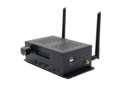
China Factory High Quality Multi
Specifications: Layers: 2Thickness: 0.6-1.6mmMaterial: FR4 KB6160Size: 115*62mmSurface treatment: HASL/OSP/IMMERSION GOL
Send your inquiryDESCRIPTION
Basic Info.
| Base Material | Copper |
| Insulation Materials | Epoxy Resin |
| Model | PCB |
| Brand | Shengyi, Kb, Nanya, Ilm |
| Impedance | 50/90/100 Ohm |
| Surfaec Treatment | HASL |
| Trace Width(Min.) | 4mil |
| Hole Sizes | 0.25mm |
| Bevel Edge | Yes |
| Criteria | Aql II 0.65 |
| Transport Package | Vacuum Packaging |
| Specification | 115*62mm |
| Trademark | XMANDA |
| Origin | Made in China |
| HS Code | 8534009000 |
| Production Capacity | 50000sqm/Month |
Product Description
Specifications:
Layers: 2Thickness: 0.6-1.6mmMaterial: FR4 KB6160Size: 115*62mmSurface treatment: HASL/OSP/IMMERSION GOLDLine width/spacing: 5/5milMinimum aperture: 0.25mmSolder mask color: yellowFinished copper thickness: 1/1 OZFeatures:
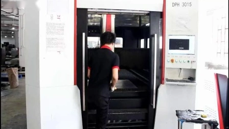
1. The integration of the board design is very high, the thickness-to-diameter ratio exceeds 10:1, and the difficulty of electroplating of copper is high.2. Made of TG140 materialShenzhen XMD Circuits Co.,Ltd, previously known as Jaleny(jlypcb), was founded in 2009 and started the journey of circuit board in Shenzhen,China. Through the introduction of advanced production and testing equipment and technical exchanges with factories in the same industry and engineering colleges, XMD greatly expanded the process capacity of double-sided board and multi-layer board. In 2011, we began to explore overseas markets and export foreign orders to all parts of the world. In 2018, Jiangxi Ji'an added a new production line, mainly making batch orders.
Able to produce 50,000 sqm of PCBs monthlyOne-stop solutions for clients (PCB & PCBA)Over 12 years of Experience in PCBsAvg Response time: ≤24 h (experienced Engineers to Serve you)Comply with RoHS,TS16949,ISO9001 and UL certifications.Flexibilities in Shipment Arrangement (FOB HK or Shenzhen by sea or by air, CIF via DHL,Fedex,UPS or TNT etc.)
A professional team, using automation, digitization to greatly improve pcb production efficiency and reduce PCB procurement costs.High-quality Raw Material★Traceable source of branded raw material★Standardized procurement process★Strict supplier selection policyProduction Equipment★High precision processing equipment★Efficient operation guarantees quality★Meet various special technical processesIntelligent System★Intelligent audition★Intelligent CAM★Intelligent paneling★Intelligent productionStrict Inspection★100% AOI testing★100% FQA/FQC★Quality Control★'Failed One Lost Ten'| Our Capabilities and Technology | |||
| Items | 2022 | 2023 | |
| Layers | (MP):22layer,(Sampling):32 layer | (MP):32layer | |
| Max. Board THK | Sampling 4.0mm / MP :3.2mm | Sampling 5.0mm / MP:3.2mm | |
| Min. Board THK | Sampling :0.4mm /MP :0.5mm | Sampling: 0.3mm / MP:0.4mm | |
| Base copper | Inner layer | 1/3 ~ 6OZ | 1/3~8 OZ |
| Outer layer | 1/3 ~ 6 OZ | 1/3 ~ 8 OZ | |
| Borehole diameter | Min.PTH | 0.2mm | 0.15mm |
| Max. aspect ratio | 10:01 | 12:01 | |
| HDI aspect ratio | 0.8:1 | 1:01 | |
| Tolerances | PTH | ±0.076mm | ±0.05mm |
| NPTH | ±0.05mm | ±0.03mm | |
| Solder mask opening | 0.05mm | 0.03mm | |
| Solder dam | (Green) 0.076mm , | (Green) 0.076mm , | |
| (other color) 0.1mm | (other color) 0.08mm | ||
| Min. core THK. | 0.1mm | 0.08mm | |
| Bow&twist | ≤0.5% | ≤0.5% | |
| Routing Tol. | Sampling :±0.075mm /MP:±0.1mm | Sampling:±0.075mm /MP:±0.075mm | |
| Impedance Tol. | ±10% | ±8% | |
| Min. w/s (Inner layer) | 0.075 / 0.075mm | 0.075 / 0.075mm | |
| Min. w/s (Outer layer) | 0.075 / 0.075mm | 0.075 / 0.075mm | |
| (Min. BGA size) | 0.2mm | 0.15mm | |
| (pitch)(Min. BGA Pitch) | 0.65mm | 0.5mm | |
| (Working panel size) | 600mm*700mm | 600mm*700mm | |
| Special process | Split gold fingers, Counter-bore , Counter-sink, Back-Drill, POFV , Mech. Drilling Blind hole. | ||